Learning Assembly — Part 3
How do Processors Actually Work?
Looking at the internals of the 6502 microprocessor will allow us to better understand the code we write.
A microprocessor has a very important role inside your computer. Fabricated on a single chip, it has the responsibility of controlling the functions of the machine. In this article, we will look specifically at the MOS Technology 6502, an incredibly popular chip from the seventies. Though the technology is old, a lot of what we will say will be applicable to modern machines too. This article also doubles as part 3 in my learning assembly series (Part 1, 2). However, I aim to make each piece as standalone as possible — there might be a few things that rely on the previous parts, but if all you’re interested in is how a microprocessor works hopefully this piece is still for you!
The 6502 (sixty-five-oh-two)
From the perspective of learning the 6502 Assembly language, we can recall that is strongly linked to the architecture it is written on. Everything you write will, on some level, depend on the instruction set and hardware of the processor. To write a program you may not require a deep knowledge of how the 6502 works, but to write an efficient one you will. We have begun to see this already. In the first part of this series, we saw how instructions can be different on different machines and in Part 2 we saw how the hardware enables us to compute things more easily. We will start to be able to piece everything we have learned so far together. As we continue in the following weeks we will be able to refer back to here as well, and further appreciate the links between the hardware and software we come to write.
To understand the architecture of a microprocessor this article will centre around the following figure:

This is the layout of a standard microprocessor of the era. Let's go through it bit by bit, trying to understand it all.
Data Buses
We will begin outside of the 6502 microprocessor unit (MPU), with the data buses. A computer bus has the job of transferring data and signal around the machine. For a 6502, they are three of them:
- The data-bus: As the name might suggest, this transfers data around. The data-bus is 8-bits wide, which means it can only carry 8 bits at a time. If you want to carry more data than that two separate signals will have to be sent down the bus. This means you can transfer the number
00011000in one trip, but00110001 00110101will take two. Usually, it will carry data from memory to the MPU, from the MPU to memory, or the MPU to an Input/ Output device. - The address-bus: This bus carries addresses. These address will usually be a source, or a destination, for data. The address bus also differs from the data-bus as it is 16-bits wide. This means you can access any 16-bit address. Practically, this means you only have access to ~64000 addresses. After you have stored something in them all, that’s it! No more memory! Interestingly, this has been a problem up to quite recently — even modern 32-bit computers can only natively access around 3gb of ram (this problem is called the 3gb barrier).
- The control-bus: The control bus will try to keep everything inside the machine synced up. Here, it has been removed for simplicity.
MPU and Registers
The microprocessor (MPU) in the above figure, in our case, is the 6502. It contains the arithmetic-logical-unit (ALU), the control-unit (CU) and the registers (some of which are the flags we saw in week 2). The CU has control over how the processor operates. It decides when it receives an instruction, data or an address how to interpret it.
Below, is a figure showing the internals of the 6502 (sans the CU). Outside of this, it will also require precise timing. This is why it is connected to a timer in the above figure.

Let’s go through this diagram, right to left, and discuss what is going on.
The ALU has a recognisable ‘V’ shape. Its role in the 6502 is to perform the calculations. It will accept two inputs, one in the ‘left input’ and one into the ‘right input’. With this, you can do addition (the ADC instruction) or subtraction (the SBC instruction). The left input of the ALU is connected to the accumulator, the A register. When doing logical or arithmetic operations usually one of the values is stored in the accumulator and the other somewhere in memory. The result of whatever operation will then also, usually, be stored in the accumulator. It is after this accumulating behaviour that the register gets its name.
The next two parts are the 8-bit X and Y registers. These are used frequently as ways to store values. They are useful as the 6502 comes with several instructions to manipulate them. Among these are INX which will increment the value in X up by 1, DEY which reduces Y by 1 and TXA which transfers the contents of X to A. Having this variety registers gives us ways to move and modify data without having to specify a memory location. We will later this article see that this can improve the speed of the code we write.
Then, there is a range of registers stored in P:
- N: keeps track if the result in the ALU is negative.
- V: the overflow flag (remember, from last week!)
- B: used to handle breaks (we will discuss this more in a later post).
- D: this helps handle BCD numbers. This is a different way to represent data. We will not discuss it here.
- I: this tracks how interrupts will be handled (we will discuss this more in a later post).
- Z: keeps track if the result of a calculation is zero.
- C: the carry flag (from last week as well!)
Having all these registers allow us to keep track of data and make comparisons. For example, we might want to branch to a different part of our program if the result of a calculation is zero. By checking the Z register we have a way to know if we should do this. Some of these registers make use of certain instructions (BRK sets B to 1). As we encounter these I will describe the effect on the register.
The Stack-Pointer (SP), points to a specific bit in a place in memory called the stack. Using it we can keep track of where in the stack we are. I will go into more detail about this when we discuss the stack later in this post.
Whatever program we write will have to be kept somewhere in memory. As we run it, we will have to identify where in memory each instruction is and pass it to the processor to be interpreted and executed. The Program-Counter (PC) is a 16-bit registry. By checking here we should be able to learn the location of the next instruction the program will need to carry out. Let’s look more into this right now!
Instructions and the Program Counter
As we run a program the processor will be in a constant cycle of fetching instructions then decoding and executing them.
Fetch: In this step, the contents of the program counter (PC) are deposited onto the address bus. By checking here we should be able to learn the next instruction the program will need to carry out. This will then be deposited in a special internal register called the instruction-register (IR). The fetch cycle is now finished!
Decode and execute: With the appropriate instruction in the IR, the control unit (CU) can begin to decode it. At this point, it can generate the signals needed to carry out the instruction. The length of time this takes will differ depending on what is being generated. Some instructions can happen inside the MPU (for example, INX), whereas some will need something else from memory (ie, data or a memory address). The latter type of instruction will take longer, as you need to take a trip to somewhere in memory to compute it. It’s worth then writing code in a way that will use the first type of instruction. The time it takes to do an instruction is measured in clock cycles. The 6502 uses a one-megahertz clock, therefore a clock cycle takes 1 microsecond.
Finally, the PC will be incremented so it points to the next instruction. Now, the process can begin again.
Memory Maps
We have discussed how with a 16-bit address bus we can reach 65,535 different locations in memory. While we access each of these addresses with the same methods that does not mean that every section of memory is used for the same purpose. The 64,535 addresses are divided into pages. Each page is a block of 256. This means that from address 0 to 255 (or 0 to 100 in hexadecimal) is page 0, address 256 to 511 is page 1, and so on. In your code you will, therefore, be tracking the page you are on and your location within a page. As you cross a page boundary (eg, go from page 12 to 13) it can result in needing to execute an extra instruction. This is because you are not just updating your location within the page, but the page number as well.
Certain pages within the 6502’s memory are there to perform specific tasks. A memory map is a figure that describes how the locations in your system are meant to be used. Regardless of what 6502 system you are using (Apple ii, c64, NES, etc..) a lot of the functionality will be the same. However, the memory map can be different. Below is a very generic 6502 memory map
Zero Page
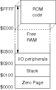
The first page in the 6502 has an important position. The zero-page, which ranges from 0 to 255, is the only area in memory that can be accessed with an 8-bit address. Since parsing an 8-bit address is quicker than parsing a 16-bit one, the zero-page becomes an area in memory where data can be read and written to more efficiently. Therefore, it is sensible to store important data there that will need to be read a lot.
The Stack
The second page is also very important. The Stack ranges from 256 to 511. This area of memory is a last-in-first-out (LIFO) list. Effectively, this means that you can only retrieve from the stack the last thing you deposited into it. It is like a neat pile of papers on a desk, you can only ever access the top one. We then have a stack pointer (the register S) that points us to the memory address that corresponds to the top of this pile. The 6502 even gives us some manual control, allowing us to push and pull things to the stack at will using PHA and PLA. It might seem strange why you would want an area of memory like this. Let's try to give an example where it would be useful.
Firstly, some terminology — we will call a set of instructions we use a lot a subroutine. You could imagine this kinda like a function you would write in Python. Now, let's write a bit of pseudocode:
1. a = 1
2. b = 2
3.
4. c = subroutine1()
5. x = a + b + c
6.
7. subroutine1:
8.     y = subroutine2()
9.     return y
10. subroutine2:
11.     z = 2
12.     return z
We will imagine the numbers we see on the left side to be locations in memory. At memory location 1 a = 1 will be stored, and so on. As we go through each line our program counter will be incremented upward, so we know what will happen next. However, eventually, we will get to line 4 and we will have to call subroutine1(). To resolve this, we will have to jump to line 7. When this subroutine is over, how will we know how to get back home to line 5?
What will happen, to ensure this information is retrievable, is that the location where we will need to return will be pushed to the stack. We can now continue as normal from line 7, knowing that when we hit a return statement we can pull that information from the stack, add the location of line 5 to the program counter, and return home.
However, the example gets a little bit more complicated here. When we reach line 8 (inside subroutine1) we now have to enter subroutine2() at line 10. Automatically, the location of line 9 (where we will have to return to) will be pushed to the stack. The contents of the stack now look like this:
1. line9
2. line5
The location of line 9 is the last thing we pushed in, and therefore it will have to be the first thing we retrieve from it. As we will see though that will be the exact behaviour we want.
So, we are now at line 10 and inside subroutine2(). We can progress like normal to line 12. At line 12 the subroutine ends and we get a return statement. What should we do? Where do we go next? At this point, by pulling out the location at the top of the stack we know to go back to line 9.
Now that we are line 9 again we see this is another return statement. Let's pull from the stack again and get the location of line 5. The program will now jump back here and finish.
It’s a really neat idea, and worth trying to get your head around. To very quickly sum it up (in my mind at least) the stack can be used as a way for your machine to “drop breadcrumbs”. By saving where it will need to return too, once it gets “lost” in a subroutine the LIFO mechanism of the stack guarantees it can find its way home.
Imagine for a moment however you kept entering subroutines. You would never get a chance to remove something from the stack. Eventually, the stack would fill with locations and run out of space, causing a crash. This is called a Stack Overflow (hey! that's the name of that website!).
I/O
The next page is reserved for I/O devices. Accessing these areas of memory will allow us to interact with the outside world. Data here would correspond to external devices. Reading and writing to these memory locations would allow us to communicate with printers, game controllers and other peripherals.
RAM
In this diagram, the Random Access Memory (RAM) is mapped to $0300 to $E000 (these are hex values, remember!). This is an area we can write data to.
ROM
The locations between $E000 and $FFFF are mapped to Read Only Memory (ROM). As the name suggests, we cannot write to here. In fact, any attempt to do so will simply be ignored. An example of ROM would be data stored on a game cartridge. As the console is booted up this memory can be read, but obviously cannot be written to or else the game data would be changed. If you wanted to modify something in ROM it would first need to be transferred into RAM.
It is up to us, the programmers, to keep track of where the data is stored and if it is stored appropriately. As we change from system to system we will also need to be aware that memory may be mapped differently.
We will end the discussion on memory with a slightly different topic: endianness. Whether a processor and language are little-endian or big-endian is based on how it orders bytes within a number. For example, a little-endian system will place the most significant bit of a number on the right. It takes 2 bytes to store the hexadecimal number ABCD. As the 6502 is little-endian the 2 bytes will, therefore, be ordered: CD, AB. Big-endian machines do the opposite. This will become important as we start to write code ourselves.
Conclusions
This week we have had a look at the main parts of the 6502’s hardware, showing us how a microprocessor works in the process. What is important for us right now is the large range of registers and the memory map that the 6502 gives us. These have a very strong impact on what we can do with the machine. As we delve into the instruction set and write programs ourselves we will see how interlinked our software will be to the hardware. At the moment it might seem like we have learned a lot of different and unrelated ideas but as we progress we will see how it all fits together.
Now, with knowledge of the hardware and how data is represented, we will move onto writing some code! Next time, a set of simple programs will be shown to broaden our knowledge of the instruction set and allow us to get a better idea of how Assembly language is written.
This is the third in my “learning assembly” series.
- Part 1: Introduction to 6502 Assembly
- Part 2: Get to Grips with Binary Numbers
- Part 3: How do Processors work?
- Part 4.1: Let’s Write Some Assembly!
- Part 4.2: Let’s Write Some (Harder) Assembly!
- Part 5: The Apple ii
This article has been adapted from my personal blog. Most of the content I talk about will come from two main sources: “6502 Assembly Language Programming” by Lance A.Leventhal and “Programming the 6502” by Rodney Zaks.